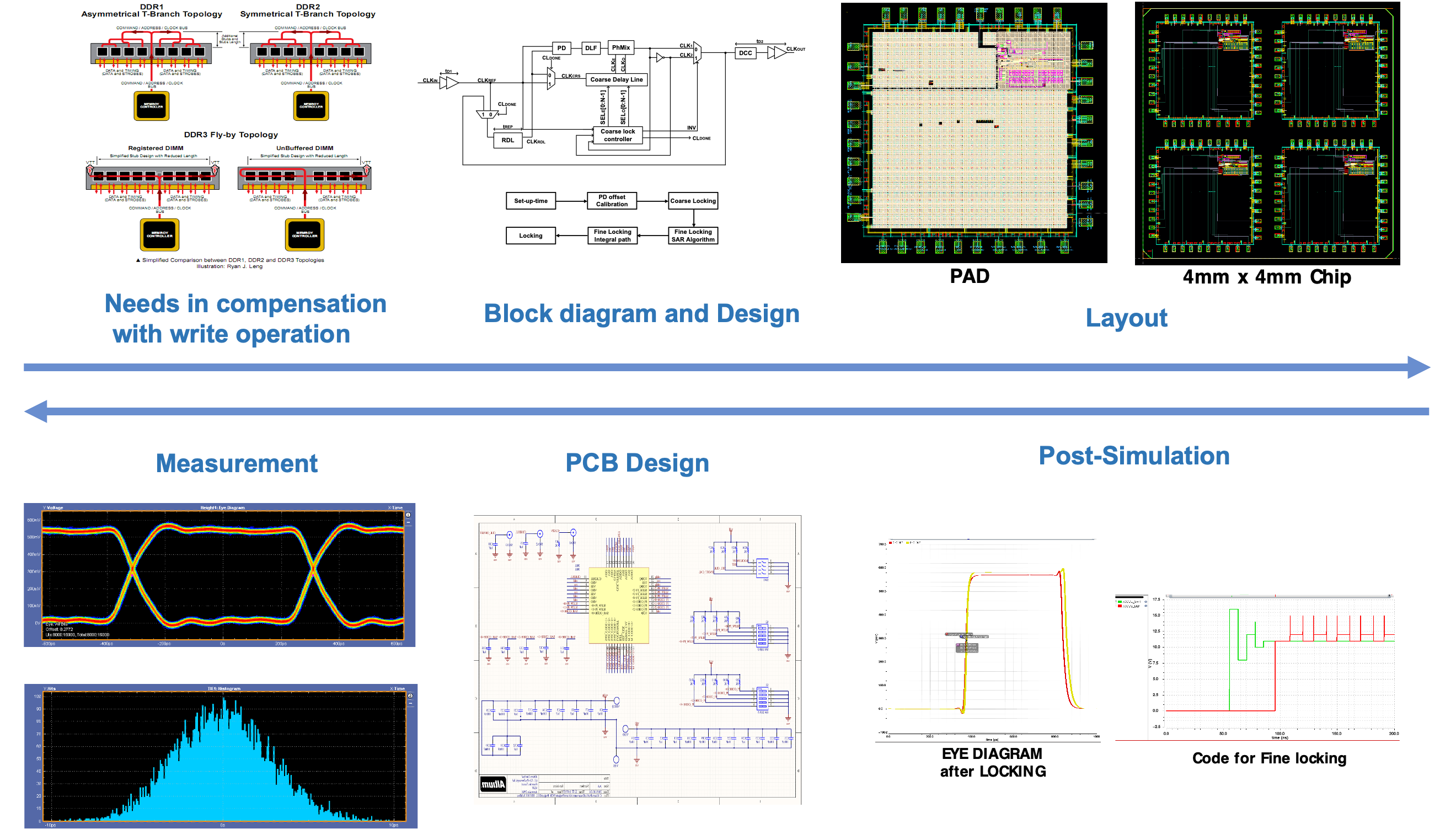
When designing the interface circuit between Memory and CPU, this circuit needs another block related to a different clock. Since not only two components but also every hardware had its clock rate, this independent circuit shoud need a synchronization when writing the data. For this reason, I started to design this circuit named Delay Locked Loop(DLL) after creating the PHY interface block.

The procedure of Delay Locked Loop
Specifically, this circuit gives the sychronized clock for the next destination, such as the CPU. The logic diagram constituted as Coarse and Fine control. The Coarse control has a delay cell constituted by NAND and NOT gate, and a counting cell named Ring-counter, a group of D-flip flops. After the difference between the target clock and the tuning clock is under the range, it goes to fine-tuning seamlessly. This fine control includes phase interpolation, a digital loop filter for controlling the circuits, and a phase detector for judging the correct timing for synchronization. We verificed the circuit performance by simulating in process, temperature, and voltage. After designing the circuits, the layout, PCB design and estimation were as follows. The abstract application is as below.
Application
- Coarse and Fine control line
- Inverter-based-phase interpolation in fine control
- Digital Loop Filter with SAR decision circuit
- Phase rotating
- Self-calibrated offset Phase Detector with digital method
Link
- This project had a poster in 19th RF/Analog Circuit Workshop.
- Poster and Paper in 19th RF/Analog Circuit Workshop