This project started from the need to design the interface circuit between the CPU and Memory. Since not only two components but also every hardware had its clock rate, the independent circuit for synchronization is necessary. For this reason, the independent circuit for receiving and transceiving the amount of data between CPU and Memory is essential, named the PHY interface.
The procedure of PHY Interface
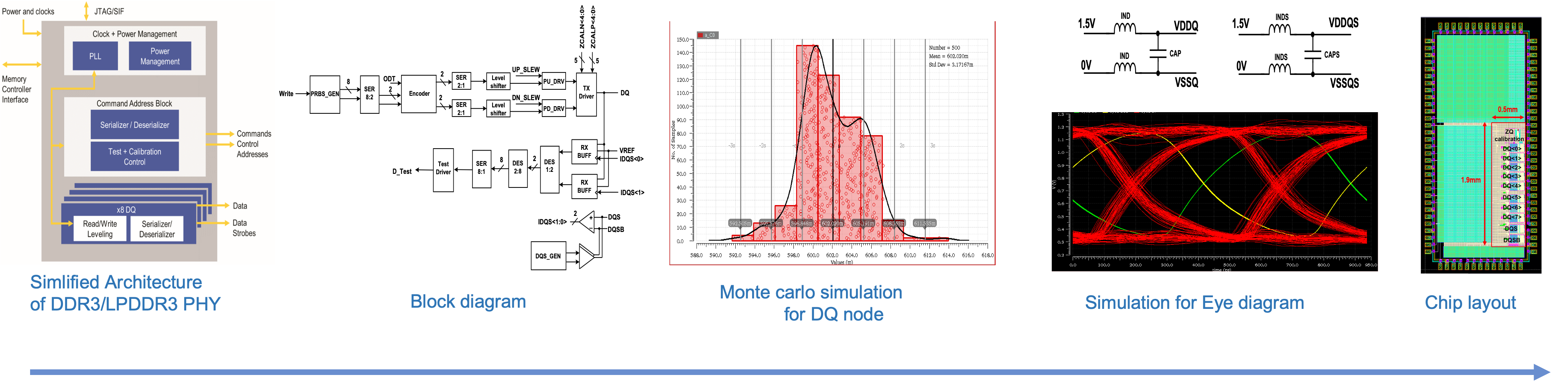
In this project, I supported The design procedure including specifications, circuit design, verification with PVT(Process, Voltage, and Temperature) variation, Layout, and design/estimate PCB board. Specifically, it targeted DDR3 and LPDDR3 memory specifications referred to as JEDEC Standard. The component constituted the list as below.
Application
- Serializer/Deserializer
- ZQ Calibration targeting error rate 3%
- Predriver for adjusting slew rate and write operation
- Estimation of Eye diagram in Tx
- Rx buffer for sampling